Wydawcy
Katalog tematyczny
- Archeologia (109)
- Ekonomia, finanse, business (13704)
- Filozofia (1445)
- Historia (3040)
- Języki i językoznawstwo (2356)
- Lifestyle, hobby i rozrywka (475)
- Medycyna (9704)
- Nauki humanistyczne (4)
- Nauki o Ziemi i środowisku (2638)
- Nauki ścisłe (20412)
- Nauki społeczne (8486)
- Nauki techniczne (13450)
- Prawo (1696)
- Publikacje informacyjne i interdyscyplinarne (1288)
- Religia i wierzenia (917)
- Technika komputerowa (4067)
- Zdrowie, relacje międzyludzkie i rozwój osobisty (657)
Informacje szczegółowe o książce

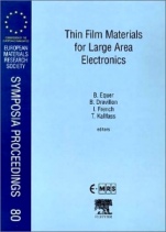
Thin Film Materials for Large Area Electronics
ISBN 9780080436074
Autor: Equer, B.Drevillon, B.French, I.Kallfass, T.
Wydawca: Elsevier
Dostępność: 3-6 tygodni
Cena: 749,70 zł
Przed złożeniem zamówienia prosimy o kontakt mailowy celem potwierdzenia ceny.
ISBN13: |
9780080436074 |
ISBN10: |
0080436072 |
Autor: |
Equer, B.Drevillon, B.French, I.Kallfass, T. |
Oprawa: |
Hardback |
Rok Wydania: |
1999-03-17 |
Tematy: |
TJFD5 |
The symposium brought together more than a hundred attendees from many countries including a significant participation from Japan and other East-Asia countries. Many of the trends observed in the 1st Symposium held in 1996 were confirmed: displays are indeed the main application in LAE (photovoltaics were not included in the topics of this symposium) and active matrix display (AMLCD) is still the leading technology. Future AMLCDs integrating the display drivers onto the same substrate require much faster thin-film transistors (TFTs) than those used for LCD addressing, therefore putting a strong demand on polysilicon performances. As a consequence the quest for an improved low temperature, large area (and low cost) polysilicon process is intensive and the competitors, including direct plasma deposition and excimer laser crystallization of amorphous layers, are reporting significant steps forward. With the tremendous demand for efficient colour flat panel displays, other display technologies are gaining interest. Field emission display (FED) is one of them. FEDs based on amorphous tetrahedral carbon thin-films are stimulating intensive studies on the optoelectronic properties of this complex material.
Large area pixellized sensors for x-ray radiography and document scanning is another field of application in LAE which has recently reached initial production. Using a TFT or diode pixel addressing similar to AMLCD, this kind of device benefits from most of the AMLCD technology. However these devices present an increased complexity and stringent specifications on noise which in turn means materials with improved electronic transport properties. Finally, LAE is a fast developing area in thin-film research and technology. Initially an all-silicon domain, it now involves a large range of thin-film semiconductors and dielectrics, whose properties need to be fully understood and for which flexible and efficient processes have still to be developed.
Selected papers: Preface. Growth mechanism of microcrystalline silicon obtained from reactive plasmas (A. Matsuda). Properties of polycrystalline silicon films prepared from fluorinated precursors (S. Ray et al.). Microcrystalline silicon growth on a-Si:H: effects of hydrogen (P. Roca i Cabarrocas, S. Hamma). Carrier transport, structure and orientation in polycrystalline silicon on glass (K. Nakahata et al.). Solid-phase crystallization of amorphous SiGe films deposited by LPCVD on SiO
Koszyk
Książek w koszyku: 0 szt.
Wartość zakupów: 0,00 zł
Informacje
Kontakt
Gambit
Centrum Oprogramowania
i Szkoleń Sp. z o.o.
Al. Pokoju 29b/22-24
31-564 Kraków
Siedziba Księgarni
ul. Kordylewskiego 1
31-542 Kraków
+48 12 410 5991
+48 12 410 5987
+48 12 410 5989
Subskrypcje
Administratorem danych osobowych jest firma Gambit COiS Sp. z o.o. Na podany adres będzie wysyłany wyłącznie biuletyn informacyjny.

© Copyright 2012: GAMBIT COiS Sp. z o.o. Wszelkie prawa zastrzeżone.
Projekt i wykonanie: Alchemia Studio Reklamy


